Upgrade & Secure Your Future with DevOps, SRE, DevSecOps, MLOps!
We spend hours scrolling social media and waste money on things we forget, but won’t spend 30 minutes a day earning certifications that can change our lives.
Master in DevOps, SRE, DevSecOps & MLOps by DevOps School!
Learn from Guru Rajesh Kumar and double your salary in just one year.
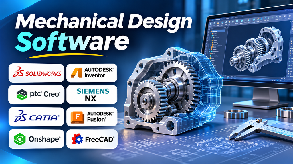
Electronic design automation software sits at the center of modern electronics development. From a simple printed circuit board (PCB) for an embedded device to a complex system-on-chip (SoC), engineers use EDA tools to translate electrical requirements into designs that can be simulated, verified, manufactured, and tested.
The challenge is that EDA is not one application or one workflow. Schematic capture, PCB layout, analog simulation, digital logic synthesis, formal verification, and semiconductor physical design are different engineering tasks. A tool that excels at PCB routing may have little relevance to verifying a processor’s logic, while an integrated-circuit design platform may be excessive for a small electronics project.
Choosing effectively starts with understanding which part of the design process needs support, how much complexity the project involves, and which file formats and manufacturing workflows must be supported.
What Electronic Design Automation Software Actually Does
EDA software helps engineers design and verify electronic systems before committing to physical production. Depending on the product, it may support one or more of these activities:
- Schematic capture: Creating circuit diagrams and defining component connections.
- PCB design: Arranging components and routing electrical connections across circuit-board layers.
- Circuit simulation: Predicting circuit behavior using mathematical models, including analog and mixed-signal simulation.
- Digital design and verification: Describing digital logic, simulating behavior, checking correctness, and verifying timing.
- IC synthesis and physical design: Transforming a digital hardware description into a gate-level implementation and preparing it for semiconductor fabrication.
- Design rule checking: Identifying violations of electrical, geometric, manufacturing, or technology-specific constraints.
- Signal and power integrity analysis: Evaluating effects such as crosstalk, voltage drop, and high-speed signal behavior.
These capabilities often come from separate applications that exchange design data. Some vendors provide integrated environments, while other workflows combine tools from multiple suppliers.
The Main EDA Tools and Where They Fit
The following products represent different parts of the electronic design market rather than a single interchangeable shortlist.
1. Altium Designer — For professional PCB design
Altium Designer brings schematic capture, PCB layout, component management, and design-rule workflows into a commercial design environment. It is particularly relevant to teams developing multi-layer boards that need consistent electrical and physical design data.
Its main consideration is the cost of commercial licensing and the effort required to establish disciplined libraries, constraints, and collaboration practices. Before adopting it, confirm that the licensing arrangement, collaboration features, and manufacturing outputs fit your team.
2. Cadence OrCAD X — For schematic-driven PCB engineering
OrCAD X serves engineers designing electronic circuits and printed circuit boards. It is worth evaluating when schematic accuracy, constraints, and a structured PCB design workflow are central to the project.
OrCAD is part of Cadence’s broader electronic design ecosystem. Product editions and available capabilities differ, so compare the precise package being offered rather than assuming every advanced analysis or enterprise feature is included.
3. Cadence Allegro X — For complex and high-speed PCB layouts
Allegro X is aimed at advanced PCB engineering, including demanding layout and constraint-management requirements. It becomes relevant when a design has dense component placement, many routing constraints, or complex signal-integrity considerations.
Its capabilities and learning requirements can be unnecessary for simple boards. Teams should also examine how the chosen edition works with existing Cadence libraries, design data, and verification tools.
4. Siemens PADS Professional — For engineering-focused PCB workflows
PADS Professional supports PCB design for engineers who need schematic and layout capabilities without necessarily adopting the most extensive enterprise design environment.
It is worth considering for product-development teams with established engineering processes. Evaluate the exact configuration, library-management approach, collaboration requirements, and compatibility with your manufacturing partners before selecting it.
5. KiCad — For open-source PCB design
KiCad offers schematic capture, PCB layout, electrical rule checking, and 3D board visualization in an open-source environment. It is a strong candidate for individual engineers, educational projects, hobby electronics, and professional teams that want control over their design files without a conventional per-seat commercial license.
Its open-source model does not eliminate engineering work: teams still need to maintain accurate symbols and footprints, review design rules, verify manufacturability, and manage collaboration. Advanced enterprise integrations may require additional tools or process development.
6. Autodesk Fusion — For electronics and mechanical product development
Fusion combines mechanical product design with electronics design capabilities, making it useful when a PCB must fit into an enclosure or interact closely with mechanical components.
The advantage is the opportunity to coordinate board and enclosure design within a connected workflow. Check the specific subscription, data-management arrangements, offline requirements, and exchange formats before committing to it for production work.
7. LTspice — For analog circuit simulation
LTspice is a SPICE-based circuit simulator used to analyze electronic circuits and inspect simulated waveforms. It is especially useful for investigating power supplies, switching converters, filters, and other analog circuits before building prototypes.
Simulation quality depends on the circuit model, component parameters, solver settings, and assumptions. A simulation result is not a guarantee of real-world behavior, especially where parasitics, thermal effects, component tolerances, and layout-dependent behavior matter.
8. Cadence Virtuoso — For custom integrated-circuit design
Virtuoso is associated with custom IC design, including transistor-level schematic work, analog and mixed-signal layout, and related verification workflows. It serves a different purpose from PCB design software: the engineering object is an integrated circuit implemented using semiconductor process technologies.
Adoption depends on process design kits (PDKs), foundry requirements, licensing, and the verification tools available to the design team. It is generally not the right starting point for a conventional PCB-only project.
9. Synopsys Design Compiler — For digital logic synthesis
Design Compiler is used in digital IC implementation workflows to synthesize RTL descriptions into gate-level logic under specified timing, power, and area constraints.
Its relevance is greatest for semiconductor teams designing digital hardware, not for engineers simply laying out a circuit board. Results depend on the RTL, constraints, target technology libraries, and downstream implementation flow.
10. AMD Vivado Design Suite — For FPGA-based digital systems
Vivado supports FPGA development workflows, including hardware design entry, synthesis, implementation, and timing analysis for supported AMD FPGA devices.
It is a device-family-specific engineering environment, not a general-purpose replacement for PCB CAD or custom IC design tools. Device compatibility, licensing options, resource constraints, and the target board should guide the decision.
Compare Tools by Engineering Task, Not by Brand
| Tool | Primary role | Typical project |
|---|---|---|
| Altium Designer | PCB design | Commercial electronic products |
| Cadence OrCAD X | Schematic and PCB design | Engineering-led circuit-board development |
| Cadence Allegro X | Advanced PCB layout | Dense, complex, high-speed boards |
| Siemens PADS Professional | PCB design | Professional product electronics |
| KiCad | Open-source PCB design | Prototypes, education, and production boards |
| Autodesk Fusion | Mechanical and electronics design | Products combining PCBs and enclosures |
| LTspice | Circuit simulation | Analog circuits and power electronics |
| Cadence Virtuoso | Custom IC design | Analog and mixed-signal semiconductor design |
| Synopsys Design Compiler | Digital logic synthesis | ASIC and digital IC workflows |
| AMD Vivado | FPGA design and implementation | Programmable digital hardware |
These tools are not ranked from best to worst. Their suitability depends on the engineering task, the target technology, and the surrounding design process.
How to Select EDA Software for Your Project
Start with the final deliverable
Identify what the team must produce:
- A manufacturable PCB and its fabrication files
- A validated analog circuit
- A digital design implemented on an FPGA
- A custom integrated circuit
- A complete product that combines electronics and mechanical components
This distinction removes many unsuitable products immediately. A PCB editor will not replace an ASIC synthesis and verification flow, and an IC design platform is unnecessary for a simple sensor board.
Evaluate design complexity
A small two-layer controller board has different needs from a dense board containing high-speed memory, controlled-impedance routing, or multiple power domains.
For more demanding designs, investigate:
- Electrical and physical design-rule constraints
- Differential-pair and impedance-control workflows
- High-speed signal-integrity analysis
- Power-integrity and thermal considerations
- Multi-layer stack-up definition
- Automated checking and review capabilities
Do not pay for specialist analysis merely because it is available. Establish which risks the project actually needs to control.
Verify library and component-data management
Libraries influence the reliability of the entire design. Incorrect footprints, outdated component parameters, or inconsistent symbol assignments can create expensive manufacturing errors.
Ask how the software handles:
- Component symbols and physical footprints
- Manufacturer part numbers and lifecycle information
- Shared libraries and version control
- Custom component creation and review
- Reuse across multiple projects
- Approved component and design-rule policies
For a team, library governance can be as important as the drawing and routing interface.
Check manufacturing and interoperability requirements
Before selecting a tool, confirm that it can produce the files required by your board manufacturer, assembly house, or semiconductor flow.
For PCB production, common exchange formats include Gerber, drill files, and IPC-2581 or ODB++ where supported and required. Depending on the workflow, assembly documentation and pick-and-place outputs may also be necessary.
For integrated-circuit development, the requirements are different and may involve PDK compatibility, foundry-specific verification, timing libraries, and downstream implementation tools.
An export format appearing in a product specification does not automatically guarantee that every design attribute will transfer without loss. Test the actual exchange process.
Calculate the total cost of ownership
Software cost is only one part of an EDA budget. Consider:
- Commercial subscriptions or license fees
- Specialist simulation and analysis modules
- Compute resources for large simulations and implementations
- Training and onboarding
- Library creation and maintenance
- Data migration and workflow integration
- Support requirements and license administration
- Costs associated with redesigns caused by preventable errors
Open-source tools can reduce licensing expenditure, but engineering teams still need time for validation, library management, documentation, and process support.
Common EDA Selection Mistakes
Choosing by feature count alone. A large feature list does not prove that a tool suits a particular engineering workflow. Focus on the capabilities required for the design and manufacturing process.
Confusing simulation with physical validation. A simulated circuit can behave differently from a real board because of component tolerances, parasitics, thermal conditions, and electromagnetic effects. Use simulation as one part of verification.
Ignoring downstream manufacturing requirements. A design that looks correct in the editor may still contain footprint, clearance, drill, stack-up, or assembly problems. Validate the deliverables with the manufacturing partner.
Overlooking file ownership and portability. Understand the native project format, export options, library dependencies, and practical cost of moving a design to another environment.
Buying an enterprise platform for a simple workflow. Advanced functionality is valuable when the project needs it. Otherwise, the added cost, setup, and training may not be justified.
Questions to Ask During an EDA Software Evaluation
Before approving a purchase or standardizing a tool across a team, ask the vendor or implementation partner:
- Does the product support our exact design type and complexity?
- Which capabilities are included in the quoted license, and which require additional modules?
- Can we import our existing schematics, PCB designs, libraries, and component data?
- What manufacturing or implementation formats can it generate?
- How does it manage shared libraries, permissions, revision history, and design reviews?
- Which simulation and verification functions are native, and which depend on other products?
- What computing resources are required for our largest expected projects?
- Can we export a representative design and validate it with our manufacturing partner?
- What happens to project files and collaboration access if a subscription ends?
- What training, technical support, and migration assistance are available?
A Practical Pilot Before Committing
Choose one representative project rather than relying entirely on a vendor demonstration. It should include the components, constraints, and complexity that the team expects to encounter in real work.
Complete a small evaluation with the following checkpoints:
- Recreate or import a representative schematic.
- Validate the component library and footprints.
- Run the relevant electrical and design-rule checks.
- Complete a representative layout, simulation, or implementation task.
- Export the deliverables and have the receiving party validate them.
- Record training effort, workflow friction, and any missing capabilities.
- Confirm the licensing and operating costs for the intended team size.
Use the same acceptance criteria when comparing products. This creates a more meaningful decision than choosing whichever interface looks most impressive in a demonstration.
The Right Choice Depends on Where Your Engineering Risk Lies
For PCB-focused teams, begin by comparing Altium Designer, OrCAD X, Allegro X, PADS Professional, and KiCad against actual board complexity, library practices, and manufacturing needs. Consider Autodesk Fusion when mechanical and electronic product design must work closely together.
For analog circuit behavior, evaluate a simulator such as LTspice. For semiconductor development, choose tools that match the actual workflow: Virtuoso for custom IC design, Design Compiler for digital logic synthesis, or Vivado for supported FPGA projects.
The most effective EDA environment is not necessarily the one with the largest feature set. It is the one that supports the required engineering work, produces reliable deliverables, fits the team’s skills and infrastructure, and helps catch costly errors before they reach manufacturing.
