Upgrade & Secure Your Future with DevOps, SRE, DevSecOps, MLOps!
We spend hours scrolling social media and waste money on things we forget, but won’t spend 30 minutes a day earning certifications that can change our lives.
Master in DevOps, SRE, DevSecOps & MLOps by DevOps School!
Learn from Guru Rajesh Kumar and double your salary in just one year.
Introduction
PCB design software helps electronics engineers create printed circuit boards from idea to manufacturing. In simple words, it lets users draw circuit schematics, place components, route copper tracks, check design rules, generate fabrication files, and prepare boards for production.
PCB design matters more now because modern electronics are smaller, faster, denser, and more connected. Products such as IoT devices, electric vehicles, medical electronics, robotics, telecom hardware, industrial controllers, and consumer devices all depend on reliable PCB layouts. A poor PCB design can cause signal issues, overheating, manufacturing failure, compliance problems, or costly rework.
Common use cases include:
- Schematic capture and circuit design
- PCB layout and routing
- High-speed signal and power integrity planning
- Embedded system board design
- IoT and hardware product prototyping
- Manufacturing file generation
- ECAD-MCAD collaboration with mechanical teams
Buyers should evaluate:
- Schematic and PCB layout depth
- Design rule checking
- Component library management
- Routing tools and constraint handling
- Signal and power integrity support
- 3D PCB visualization
- Manufacturing output support
- Collaboration and version control
- Security and access control
- Pricing and learning curve
Best for: PCB designers, electronics engineers, embedded engineers, hardware startups, manufacturing teams, product companies, engineering consultants, students, educators, and enterprise electronics teams.
Not ideal for: Users who only need simple wiring diagrams, basic circuit illustrations, or non-production educational sketches. In those cases, lightweight diagram tools or beginner circuit simulators may be enough.
Key Trends in PCB Design Software
- AI-assisted PCB design is becoming more practical: Modern PCB tools are starting to support smarter routing, layout suggestions, design review assistance, and faster constraint validation.
- ECAD-MCAD collaboration is now expected: PCB teams need to work closely with mechanical teams to check board shape, connectors, enclosure clearance, thermal zones, and 3D fit.
- Cloud collaboration is growing: More teams want browser access, shared project workspaces, version history, comments, and review workflows for distributed hardware teams.
- Component data quality is becoming critical: Supply-chain risk has made component availability, lifecycle status, alternates, and library control more important than ever.
- High-speed design requirements are increasing: More boards now include fast interfaces, RF sections, DDR memory, USB, PCIe, Ethernet, wireless modules, and power-sensitive designs.
- Manufacturing-ready outputs are a major focus: Teams need Gerber, ODB++, IPC-2581, BOM, pick-and-place, assembly drawings, and clear fabrication documentation.
- Security and IP protection matter more: PCB files contain valuable product IP, so companies now review permissions, secure sharing, encryption, audit logs, and access control.
- Open-source PCB tools are more accepted: KiCad and similar tools are now used by hobbyists, startups, educators, and even some professional teams for cost-effective design work.
- Subscription pricing is common: Many commercial tools now use subscriptions, cloud services, add-ons, or tier-based plans, so buyers must review total cost carefully.
- Simulation and validation are moving earlier: Teams want to catch electrical, thermal, and manufacturability issues before ordering prototypes.
How We Selected These Tools
The tools below were selected using a practical buyer-focused evaluation method:
- Strong market recognition in PCB design and electronics engineering
- Capability across schematic capture, PCB layout, routing, and manufacturing outputs
- Fit for different segments, including freelancers, SMBs, startups, enterprises, and education
- Support for modern workflows such as ECAD-MCAD collaboration and cloud sharing
- Availability of component libraries, design rules, simulation, or analysis features
- Reliability and performance for real PCB projects
- Ecosystem strength, including integrations, APIs, add-ons, and fabrication workflows
- Security and team collaboration signals where available
- Documentation, onboarding, training, and community availability
- Balanced coverage of premium, mid-market, web-based, and open-source PCB tools
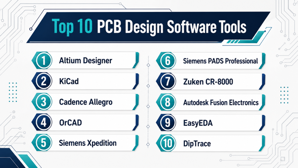
Top 10 PCB Design Software Tools
#1 — Altium Designer
Short description (2–3 lines): Altium Designer is a professional PCB design platform used for schematic capture, PCB layout, routing, 3D visualization, library management, and manufacturing preparation. It is best for professional PCB designers, hardware teams, electronics companies, and product engineering teams.
Key Features
- Unified schematic and PCB layout environment
- Advanced routing and design rule management
- 3D PCB visualization and mechanical checks
- Component and library management
- Manufacturing output generation
- ECAD-MCAD collaboration support
- Cloud-connected collaboration through Altium ecosystem options
Pros
- Strong professional PCB design workflow
- Good balance of usability and advanced features
- Helpful for complex boards and product teams
Cons
- Pricing can be high for freelancers or very small teams
- Advanced features may require training
- Best value comes when teams use the full ecosystem
Platforms / Deployment
Windows
Cloud-connected desktop / Hybrid options vary by plan
Security & Compliance
SSO/SAML, MFA, encryption, audit logs, RBAC: Varies by plan and platform configuration.
SOC 2, ISO 27001, GDPR, HIPAA: Not publicly stated.
Integrations & Ecosystem
Altium has a strong PCB-centered ecosystem with component data, manufacturing handoff, and collaboration workflows. It is useful for teams that need design, review, supply-chain visibility, and mechanical coordination.
- ECAD-MCAD collaboration
- Component library workflows
- Manufacturing outputs
- Cloud project sharing
- Version and review workflows
- Mechanical CAD export support
Support & Community
Altium provides documentation, training resources, webinars, support plans, and a large professional PCB design community. Onboarding is easier than many enterprise EDA tools, but complex workflows still need practice.
#2 — KiCad
Short description (2–3 lines): KiCad is a free and open-source PCB design suite for schematic capture, PCB layout, 3D viewing, and manufacturing file generation. It is popular with students, hobbyists, startups, open-source hardware teams, and cost-conscious professionals.
Key Features
- Schematic capture
- PCB layout and routing
- 3D PCB viewer
- Symbol and footprint libraries
- Gerber and manufacturing file generation
- Plugin and extension support
- Cross-platform desktop support
Pros
- Free and open-source
- Strong community and active ecosystem
- Good for learning, prototyping, and many real PCB projects
Cons
- Enterprise collaboration features are limited
- Formal commercial support is not as strong as premium tools
- Advanced high-speed workflows may need extra expertise
Platforms / Deployment
Windows / macOS / Linux
Self-hosted desktop
Security & Compliance
SSO/SAML, MFA, encryption, audit logs, RBAC: Not publicly stated.
SOC 2, ISO 27001, GDPR, HIPAA: Not publicly stated.
Integrations & Ecosystem
KiCad has a strong open-source ecosystem and works well with external version control, community libraries, and manufacturing outputs.
- Open-source libraries
- Plugin ecosystem
- Gerber outputs
- 3D model support
- External Git workflows
- Community-maintained add-ons
Support & Community
KiCad has strong community support, forums, tutorials, documentation, and active contributors. It is one of the best options for users who want open-source PCB design without license cost.
#3 — Cadence Allegro
Short description (2–3 lines): Cadence Allegro is an enterprise-grade PCB design platform for complex boards, high-speed layouts, signal integrity, power integrity, and advanced electronics development. It is best for large engineering teams, semiconductor-linked workflows, and high-reliability product companies.
Key Features
- Advanced PCB layout and routing
- High-speed design support
- Signal and power integrity workflows
- Constraint-driven design
- Multi-layer and dense board support
- Manufacturing preparation tools
- Enterprise collaboration and design management options
Pros
- Very strong for advanced PCB design
- Good fit for enterprise electronics teams
- Deep constraint and analysis capabilities
Cons
- Expensive and complex for small teams
- Requires experienced users
- Implementation may need structured onboarding
Platforms / Deployment
Windows / Linux depending on product configuration
Self-hosted / Hybrid options vary
Security & Compliance
SSO/SAML, MFA, encryption, audit logs, RBAC: Varies by enterprise configuration.
SOC 2, ISO 27001, GDPR, HIPAA: Not publicly stated.
Integrations & Ecosystem
Cadence Allegro fits into a broad electronics design ecosystem, including simulation, verification, component workflows, and enterprise design processes.
- Cadence EDA ecosystem
- Signal integrity tools
- Power integrity workflows
- Manufacturing outputs
- Component and library management
- Enterprise design data workflows
Support & Community
Cadence provides enterprise support, documentation, training, and professional services. The platform is best suited for teams with experienced PCB designers and formal engineering processes.
#4 — OrCAD
Short description (2–3 lines): OrCAD is a professional PCB design and circuit design tool family from Cadence. It is often used by engineers who need strong schematic capture, PCB layout, simulation, and a path into more advanced Cadence workflows.
Key Features
- Schematic capture
- PCB layout
- Circuit simulation workflows
- Design rule checking
- Component and library management
- Manufacturing documentation
- Cadence ecosystem compatibility
Pros
- Strong professional PCB design capability
- More approachable than some enterprise EDA tools
- Good fit for engineering teams that may later scale into Allegro
Cons
- Licensing and packaging may need careful review
- New users may face a learning curve
- Advanced enterprise workflows may require higher-tier Cadence tools
Platforms / Deployment
Windows
Desktop / enterprise options vary
Security & Compliance
SSO/SAML, MFA, encryption, audit logs, RBAC: Varies by Cadence configuration.
SOC 2, ISO 27001, GDPR, HIPAA: Not publicly stated.
Integrations & Ecosystem
OrCAD benefits from Cadence’s larger PCB and electronics design ecosystem. It is useful for professional PCB teams that need stronger capability than entry-level tools.
- Cadence PCB ecosystem
- SPICE simulation workflows
- Component libraries
- Manufacturing outputs
- Allegro upgrade path
- Design validation workflows
Support & Community
OrCAD has documentation, training resources, partner support, and an established professional user base. Support depends on the license type and vendor channel.
#5 — Siemens Xpedition
Short description (2–3 lines): Siemens Xpedition is an enterprise PCB design platform for complex electronics, high-density boards, systems engineering, and manufacturing-connected workflows. It is best for large electronics teams, automotive electronics, aerospace, industrial systems, and advanced product companies.
Key Features
- Advanced PCB design and routing
- Constraint-driven design
- High-speed and high-density board support
- ECAD-MCAD collaboration
- Design data management
- Manufacturing and test workflow support
- Siemens ecosystem alignment
Pros
- Strong for enterprise PCB design
- Good connection with manufacturing and lifecycle workflows
- Suitable for complex, regulated electronics products
Cons
- More complex than tools for small teams
- Enterprise licensing can be costly
- Requires planning for full implementation value
Platforms / Deployment
Windows / enterprise environments
Self-hosted / Hybrid options vary
Security & Compliance
SSO/SAML, MFA, encryption, audit logs, RBAC: Varies by Siemens enterprise configuration.
SOC 2, ISO 27001, GDPR, HIPAA: Not publicly stated.
Integrations & Ecosystem
Xpedition is useful when PCB design must connect with mechanical design, PLM, manufacturing, and large-scale engineering governance.
- Siemens Teamcenter options
- ECAD-MCAD collaboration
- Manufacturing workflows
- Constraint management
- Design reuse
- Enterprise engineering systems
Support & Community
Siemens provides enterprise support, training, documentation, and professional services. The community is more professional and enterprise-focused than casual-user-focused.
#6 — Siemens PADS Professional
Short description (2–3 lines): Siemens PADS Professional is a PCB design solution aimed at engineers and teams that need capable PCB layout, schematic capture, constraint management, and manufacturability support without always requiring the full Xpedition-level enterprise setup.
Key Features
- Schematic capture
- PCB layout and routing
- Constraint management
- Design rule checking
- 3D visualization
- Manufacturing output support
- Siemens ecosystem connectivity
Pros
- Strong capability for SMB and mid-market PCB teams
- More approachable than some enterprise platforms
- Good fit for professional board design workflows
Cons
- May still require training for advanced use
- Some enterprise capabilities may need higher Siemens tools
- Ecosystem value depends on Siemens adoption
Platforms / Deployment
Windows
Desktop / Hybrid options vary
Security & Compliance
SSO/SAML, MFA, encryption, audit logs, RBAC: Varies by Siemens configuration.
SOC 2, ISO 27001, GDPR, HIPAA: Not publicly stated.
Integrations & Ecosystem
PADS Professional connects with Siemens design and manufacturing workflows while still serving PCB teams that need practical board design capability.
- Siemens engineering ecosystem
- ECAD-MCAD workflows
- Manufacturing outputs
- Component libraries
- Constraint management
- Design review workflows
Support & Community
Siemens provides documentation, training, and partner support. Community strength is moderate and more professional than hobby-focused.
#7 — Zuken CR-8000
Short description (2–3 lines): Zuken CR-8000 is a professional PCB and system-level electronics design platform for complex boards, multi-board products, and product-centric electronics development. It is useful for automotive, aerospace, industrial, and advanced electronics teams.
Key Features
- System-level PCB design
- Multi-board design workflows
- Advanced layout and routing
- Signal and power integrity support
- 3D product-centric design
- Constraint and design reuse management
- Manufacturing preparation workflows
Pros
- Strong for complex PCB and multi-board systems
- Useful for product-level electronics design
- Good fit for advanced engineering teams
Cons
- May be too advanced for simple PCB projects
- Smaller community than Altium or KiCad
- Implementation may require expert support
Platforms / Deployment
Windows
Desktop / enterprise options vary
Security & Compliance
SSO/SAML, MFA, encryption, audit logs, RBAC: Varies / N/A.
SOC 2, ISO 27001, GDPR, HIPAA: Not publicly stated.
Integrations & Ecosystem
Zuken CR-8000 is often used where PCB design must support complex product development, multiple boards, mechanical coordination, and manufacturing planning.
- ECAD-MCAD workflows
- Multi-board design
- Constraint management
- Manufacturing outputs
- Signal and power integrity workflows
- Enterprise engineering systems
Support & Community
Zuken provides professional documentation, training, support, and implementation services. Community resources are more specialized compared with mainstream PCB tools.
#8 — Autodesk Fusion Electronics
Short description (2–3 lines): Autodesk Fusion Electronics combines schematic capture, PCB layout, and mechanical design workflows in the Fusion environment. It is useful for hardware startups, product designers, small teams, and engineers who need electronics and enclosure design to work together.
Key Features
- Schematic capture
- PCB layout
- ECAD-MCAD integration
- 3D PCB visualization
- Component library workflows
- Manufacturing file generation
- Cloud-connected collaboration
Pros
- Strong fit for product design teams
- Useful electronics and mechanical workflow connection
- Good option for startups and prototype teams
Cons
- May not match high-end enterprise PCB tools for complex boards
- Some advanced features may depend on plan or extensions
- Cloud-connected workflow may not suit every company
Platforms / Deployment
Windows / macOS
Cloud-connected desktop
Security & Compliance
SSO/SAML, MFA, encryption, audit logs, RBAC: Varies by Autodesk account and plan configuration.
SOC 2, ISO 27001, GDPR, HIPAA: Not publicly stated.
Integrations & Ecosystem
Fusion Electronics is useful when PCB design is part of a broader product design workflow involving mechanical design, 3D modeling, prototyping, and manufacturing.
- Fusion mechanical design workflows
- Autodesk ecosystem
- PCB manufacturing outputs
- Component library workflows
- Cloud collaboration
- 3D product design workflows
Support & Community
Autodesk provides documentation, learning resources, forums, and support plans. Fusion also has a strong user base among makers, startups, educators, and product design teams.
#9 — EasyEDA
Short description (2–3 lines): EasyEDA is a browser-based PCB design tool for schematic capture, PCB layout, simulation, and quick board design. It is popular with students, makers, hobbyists, and small teams that want an easy online PCB workflow.
Key Features
- Web-based schematic capture
- Browser-based PCB layout
- Component library access
- Simulation options
- Gerber and manufacturing outputs
- Online project sharing
- Quick prototype workflow
Pros
- Easy to start without complex installation
- Good for learning and small PCB projects
- Helpful for quick prototyping workflows
Cons
- Not ideal for advanced enterprise PCB projects
- Cloud dependency may concern some teams
- Limited compared with high-end PCB design platforms
Platforms / Deployment
Web
Cloud
Security & Compliance
SSO/SAML, MFA, encryption, audit logs, RBAC: Not publicly stated.
SOC 2, ISO 27001, GDPR, HIPAA: Not publicly stated.
Integrations & Ecosystem
EasyEDA is designed for fast online PCB design and manufacturing-oriented workflows. It is simple, accessible, and useful for users who want to move quickly from schematic to board files.
- Online component libraries
- PCB fabrication workflow options
- Gerber outputs
- Browser-based project sharing
- Basic simulation workflows
- Community examples
Support & Community
EasyEDA has documentation, tutorials, community examples, and user support resources. It is beginner-friendly, but enterprise support and governance are limited.
#10 — DipTrace
Short description (2–3 lines): DipTrace is a PCB design software suite for schematic capture, PCB layout, component creation, and manufacturing file generation. It is often used by small teams, consultants, educators, and engineers who want a practical PCB tool with a manageable learning curve.
Key Features
- Schematic capture
- PCB layout and routing
- Pattern and component editors
- 3D PCB preview
- Design rule checking
- Manufacturing output generation
- Multi-sheet and hierarchical design support
Pros
- Easier learning curve than many advanced PCB tools
- Practical for small teams and consultants
- Good balance of features and usability
Cons
- Smaller ecosystem than Altium, Cadence, or Siemens
- May not be ideal for very complex enterprise boards
- Advanced collaboration features are limited
Platforms / Deployment
Windows / macOS / Linux
Self-hosted desktop
Security & Compliance
SSO/SAML, MFA, encryption, audit logs, RBAC: Not publicly stated.
SOC 2, ISO 27001, GDPR, HIPAA: Not publicly stated.
Integrations & Ecosystem
DipTrace supports standard PCB workflows and manufacturing outputs. It is suitable for users who need practical design capability without a large enterprise stack.
- Gerber outputs
- Component and pattern libraries
- 3D model support
- STEP export workflows
- Design rule checks
- Standard PCB manufacturing files
Support & Community
DipTrace provides documentation, tutorials, user support, and community resources. Its community is smaller than KiCad or Altium, but it remains useful for practical PCB design work.
Comparison Table
| Tool Name | Best For | Platform(s) Supported | Deployment (Cloud/Self-hosted/Hybrid) | Standout Feature | Public Rating |
|---|---|---|---|---|---|
| Altium Designer | Professional PCB design teams | Windows | Hybrid | Unified PCB design with 3D visualization | N/A |
| KiCad | Open-source PCB design and prototyping | Windows, macOS, Linux | Self-hosted | Free open-source PCB design suite | N/A |
| Cadence Allegro | Enterprise high-speed PCB design | Windows, Linux | Self-hosted / Hybrid | Advanced constraint-driven PCB design | N/A |
| OrCAD | Professional PCB and circuit design | Windows | Self-hosted / Hybrid options vary | Strong schematic, PCB, and simulation workflow | N/A |
| Siemens Xpedition | Complex enterprise PCB systems | Windows | Self-hosted / Hybrid | Enterprise PCB design with lifecycle workflows | N/A |
| Siemens PADS Professional | SMB and mid-market PCB teams | Windows | Self-hosted / Hybrid options vary | Professional PCB design with Siemens ecosystem | N/A |
| Zuken CR-8000 | Multi-board and system-level electronics | Windows | Self-hosted / Hybrid options vary | Product-centric multi-board design | N/A |
| Autodesk Fusion Electronics | Product teams needing ECAD-MCAD workflow | Windows, macOS | Hybrid | Electronics and mechanical design connection | N/A |
| EasyEDA | Beginners, makers, quick PCB projects | Web | Cloud | Browser-based PCB design | N/A |
| DipTrace | Small teams and consultants | Windows, macOS, Linux | Self-hosted | Practical PCB design with easier learning curve | N/A |
Evaluation & Scoring of PCB Design Software
The scoring below is comparative. It reflects practical product capability, usability, integration strength, security signals, performance, support, and value. It is not a public rating and should not be treated as a universal ranking.
| Tool Name | Core (25%) | Ease (15%) | Integrations (15%) | Security (10%) | Performance (10%) | Support (10%) | Value (15%) | Weighted Total (0–10) |
|---|---|---|---|---|---|---|---|---|
| Altium Designer | 9 | 8 | 9 | 7 | 8 | 8 | 7 | 8.15 |
| KiCad | 7 | 7 | 6 | 4 | 7 | 7 | 10 | 6.95 |
| Cadence Allegro | 10 | 5 | 9 | 8 | 9 | 9 | 5 | 8.05 |
| OrCAD | 8 | 6 | 8 | 7 | 8 | 8 | 7 | 7.45 |
| Siemens Xpedition | 10 | 5 | 9 | 8 | 9 | 8 | 5 | 7.95 |
| Siemens PADS Professional | 8 | 7 | 8 | 7 | 8 | 7 | 7 | 7.50 |
| Zuken CR-8000 | 8 | 5 | 8 | 7 | 8 | 7 | 6 | 7.05 |
| Autodesk Fusion Electronics | 7 | 8 | 8 | 7 | 7 | 8 | 8 | 7.55 |
| EasyEDA | 5 | 9 | 6 | 4 | 6 | 6 | 9 | 6.35 |
| DipTrace | 7 | 8 | 6 | 4 | 7 | 6 | 8 | 6.75 |
How to interpret the scores:
- Higher scores indicate stronger overall fit across the listed criteria, not a universal winner.
- Enterprise tools score high in depth, integrations, and performance but may score lower in ease and value.
- Open-source and low-cost tools score well for value but may need more manual setup and self-support.
- Browser-based tools are easier to start but may not fit advanced or regulated workflows.
- Buyers should use these scores as a shortlist guide, then validate with real board files and team requirements.
Which PCB Design Software Tool Is Right for You?
Solo / Freelancer
Solo PCB designers need a tool that is affordable, easy to learn, and accepted by clients or fabrication partners.
Good options include:
- KiCad for free and open-source PCB design
- EasyEDA for fast browser-based design and simple projects
- DipTrace for a manageable desktop PCB workflow
- Autodesk Fusion Electronics for product design and mechanical fit
- Altium Designer if clients expect professional Altium deliverables
Freelancers should avoid expensive enterprise platforms unless their clients specifically require Cadence, Siemens, or Zuken project files.
SMB
Small and medium businesses need reliable PCB design, good libraries, manufacturing outputs, and basic collaboration.
Good options include:
- Altium Designer for professional PCB workflows
- OrCAD for engineering teams needing schematic, PCB, and simulation capability
- Siemens PADS Professional for structured PCB design in growing teams
- Autodesk Fusion Electronics for hardware products with mechanical integration
- KiCad for cost-conscious teams with strong internal skills
SMBs should focus on training cost, library governance, design review process, and fabrication output quality.
Mid-Market
Mid-market companies usually need stronger version control, library control, ECAD-MCAD collaboration, and design process governance.
Good options include:
- Altium Designer for modern PCB design collaboration
- OrCAD for professional Cadence-connected workflows
- Siemens PADS Professional for Siemens ecosystem users
- Zuken CR-8000 for complex board and system-level design
- Autodesk Fusion Electronics for product-focused teams
Mid-market buyers should test real projects during evaluation, including multi-sheet schematics, board constraints, design reviews, and manufacturing handoff.
Enterprise
Enterprise teams often need high-speed design, large team collaboration, security controls, PLM integration, manufacturing governance, and advanced analysis.
Good options include:
- Cadence Allegro for advanced high-speed PCB design
- Siemens Xpedition for enterprise PCB and lifecycle workflows
- Zuken CR-8000 for complex multi-board systems
- Altium Designer enterprise options for distributed PCB teams
- OrCAD for teams that want a professional path into Cadence workflows
Enterprise buyers should involve engineering, IT, security, manufacturing, procurement, and compliance teams during selection.
Budget vs Premium
For budget-focused users, KiCad, EasyEDA, and DipTrace are practical choices. They work well for learning, prototyping, small boards, and many professional projects.
For premium needs, Altium Designer, Cadence Allegro, Siemens Xpedition, OrCAD, and Zuken CR-8000 are stronger choices. Premium tools make sense when board complexity, team size, analysis needs, and manufacturing risk are high.
Feature Depth vs Ease of Use
If ease of use matters most, consider EasyEDA, DipTrace, KiCad, or Autodesk Fusion Electronics.
If deep PCB engineering capability matters more, consider Altium Designer, Cadence Allegro, Siemens Xpedition, OrCAD, or Zuken CR-8000.
A simple tool can be excellent for small boards, but high-speed, RF, dense, or regulated boards usually need stronger design controls.
Integrations & Scalability
PCB design does not end at layout. Teams often need connections to mechanical CAD, component databases, PLM, ERP, simulation tools, fabrication partners, and version control systems.
Strong integration scenarios include:
- Altium Designer for PCB collaboration and ECAD-MCAD workflows
- Autodesk Fusion Electronics for combined electronics and mechanical design
- Cadence Allegro for advanced enterprise electronics workflows
- Siemens Xpedition for Siemens PLM and manufacturing ecosystem users
- KiCad for Git-based open-source workflows
- Zuken CR-8000 for multi-board and product-level design
Scalability should include project size, user permissions, library control, design reuse, review workflows, and long-term data management.
Security & Compliance Needs
PCB files often contain valuable product IP, component strategy, manufacturing data, and design details. Security is important for commercial products, regulated industries, defense suppliers, automotive electronics, medical devices, and semiconductor-related hardware.
Important security checks include:
- SSO and MFA
- Role-based access control
- Audit logs
- Encryption
- Secure sharing
- Backup and recovery
- Project-level permissions
- Vendor access controls
- Export control needs
- Internal approval workflow
For cloud-connected PCB tools, review vendor security carefully. For desktop tools, review file storage, endpoint security, access permissions, and backup controls.
Frequently Asked Questions (FAQs)
What is PCB design software?
PCB design software helps engineers create circuit schematics, design board layouts, route copper traces, check design rules, and generate manufacturing files for printed circuit boards.
Is PCB design software the same as EDA software?
PCB design software is a part of the broader EDA category. EDA may also include IC design, chip verification, FPGA design, simulation, and semiconductor workflows.
Which PCB design software is best for beginners?
KiCad, EasyEDA, DipTrace, and Autodesk Fusion Electronics are often easier for beginners. They provide practical PCB workflows without requiring deep enterprise EDA experience.
Which PCB design software is best for professionals?
Altium Designer, OrCAD, Cadence Allegro, Siemens Xpedition, Siemens PADS Professional, and Zuken CR-8000 are strong professional options. The best choice depends on board complexity, team size, and workflow needs.
Is KiCad good enough for professional PCB design?
KiCad can be good enough for many professional PCB projects, especially for startups, consultants, educators, and open-source teams. For highly complex enterprise boards, premium tools may offer stronger collaboration, analysis, and support.
What pricing models are common in PCB design software?
Common models include free open-source, perpetual licenses, subscriptions, floating licenses, named-user licenses, enterprise contracts, and feature-based add-ons. Buyers should compare total cost, not only starting price.
What are common mistakes when choosing PCB design software?
Common mistakes include choosing only by price, ignoring library management, skipping manufacturing output checks, underestimating training, and not testing real design files before buying.
How long does PCB software onboarding take?
Basic users can start quickly with beginner-friendly tools. Professional teams may need more time for libraries, templates, rules, workflows, review processes, and manufacturing standards.
Do PCB tools support collaboration?
Many modern PCB tools support collaboration, but depth varies. Some offer cloud sharing and comments, while others rely on external file systems, Git, PDM, or enterprise design management platforms.
Is cloud PCB design secure?
Cloud PCB design can be secure if the vendor provides strong access controls and the company configures them properly. Buyers should review MFA, SSO, encryption, audit logs, and permission management.
Can I switch from one PCB design tool to another?
Switching is possible, but it can be difficult because symbols, footprints, rules, libraries, and board files may not transfer perfectly. Always test migration using real project data.
What files should PCB software generate for manufacturing?
Common outputs include Gerber files, drill files, BOM, pick-and-place files, assembly drawings, fabrication notes, IPC-2581, ODB++, and 3D files depending on manufacturer requirements.
Do PCB tools integrate with mechanical CAD software?
Many professional PCB tools support ECAD-MCAD workflows, 3D board export, STEP files, enclosure checks, and mechanical collaboration. This is important when board shape, connectors, and clearance matter.
What is the best alternative to expensive PCB software?
KiCad, EasyEDA, DipTrace, and Autodesk Fusion Electronics can be practical alternatives depending on project size and complexity. For enterprise-grade high-speed boards, premium tools may still be worth the cost.
Conclusion
PCB design software is a critical part of modern electronics development, but there is no single best tool for every team. KiCad, EasyEDA, and DipTrace are strong options for learners, freelancers, startups, and budget-conscious teams. Autodesk Fusion Electronics is useful when electronics design must connect closely with mechanical product design. Altium Designer and OrCAD are strong professional choices for serious PCB work. Cadence Allegro, Siemens Xpedition, and Zuken CR-8000 are better suited for complex enterprise boards, high-speed designs, regulated products, and large engineering teams.
The best next step is to shortlist 2–3 tools, test them with real board files, review manufacturing outputs, validate component library workflows, check integrations, and confirm security requirements before making a final decision