Upgrade & Secure Your Future with DevOps, SRE, DevSecOps, MLOps!
We spend hours scrolling social media and waste money on things we forget, but won’t spend 30 minutes a day earning certifications that can change our lives.
Master in DevOps, SRE, DevSecOps & MLOps by DevOps School!
Learn from Guru Rajesh Kumar and double your salary in just one year.
Introduction
Electronic Design Automation (EDA) software helps engineers design, simulate, verify, test, and prepare electronic systems for manufacturing. In simple words, EDA software is used to build chips, printed circuit boards, integrated circuits, semiconductor devices, embedded electronics, and complex electronic products before they are physically produced.
EDA matters now because electronics are becoming more complex, smaller, faster, and more software-driven. AI chips, electric vehicles, IoT devices, medical electronics, telecom hardware, aerospace systems, and consumer devices all need reliable design flows. A small design error can lead to expensive rework, failed prototypes, delays, or compliance problems.
Common use cases include:
- IC and SoC design
- PCB schematic capture and board layout
- Circuit simulation and signal integrity analysis
- FPGA and ASIC verification
- Power, performance, and area optimization
- Design rule checking and manufacturing preparation
- Hardware security and lifecycle validation
Buyers should evaluate:
- PCB or IC design depth
- Simulation and verification capabilities
- Design rule checking
- Library and component management
- Collaboration and version control
- Cloud or desktop deployment
- Integration with PLM, MCAD, and manufacturing systems
- Security and IP protection
- Learning curve and support quality
- Total cost of ownership
Best for: Semiconductor companies, PCB design teams, electronics manufacturers, hardware startups, embedded system teams, automotive electronics teams, aerospace suppliers, telecom companies, research labs, and engineering service providers.
Not ideal for: Users who only need basic electrical diagrams, simple wiring sketches, or non-production circuit illustrations. In those cases, lightweight diagram tools, simple PCB apps, or educational circuit simulators may be enough.
Key Trends in Electronic Design Automation (EDA) Software
- AI-assisted chip and board design is becoming more practical: EDA vendors are adding AI-driven optimization, faster verification, intelligent routing, design-space exploration, and productivity assistants.
- EDA and simulation are moving closer together: Electronics teams want stronger connections between chip design, thermal analysis, power integrity, signal integrity, mechanical fit, and system-level simulation.
- Cloud and hybrid EDA workflows are growing: Large teams still use high-performance on-premise environments, but cloud bursting, remote collaboration, and browser-based PCB design are becoming more common.
- Hardware security is now a design requirement: Buyers are paying more attention to IP protection, secure collaboration, access control, audit logs, and supply-chain risk.
- Chiplet and advanced packaging workflows are gaining importance: Modern semiconductor design is no longer limited to one monolithic chip. EDA tools increasingly support multi-die, package-aware, and system-level design flows.
- PCB and mechanical design integration is improving: Electronics products need better ECAD-MCAD collaboration, 3D board visualization, enclosure checks, connector clearance validation, and thermal planning.
- Verification complexity is increasing: ASIC, SoC, FPGA, and safety-critical electronics projects need stronger verification, formal analysis, emulation, and compliance-ready documentation.
- Open-source EDA continues to mature: Open-source tools are not replacing enterprise EDA for advanced chip design, but they are becoming more useful for education, research, prototyping, and community-driven hardware projects.
- Subscription and token-based licensing remain important: Buyers need to carefully evaluate license flexibility, floating licenses, cloud compute costs, support plans, and long-term renewal pricing.
- Interoperability is a serious buying factor: Teams need support for Gerber, ODB++, IPC-2581, SPICE, Verilog, VHDL, SystemVerilog, STEP, DXF, and other common formats depending on the design flow.
How We Selected These Tools
The tools below were selected using a practical EDA buyer-focused methodology:
- Strong market adoption and recognition in PCB, IC, semiconductor, or electronics design
- Feature completeness across schematic capture, layout, simulation, verification, or manufacturing outputs
- Suitability for different user groups, including enterprises, SMBs, startups, researchers, and open-source users
- Reliability and performance signals for complex electronics workflows
- Ecosystem strength, including libraries, IP, integrations, APIs, and partner networks
- Security posture signals such as enterprise administration, access control, and collaboration governance
- Fit for modern workflows such as AI-assisted design, cloud collaboration, and advanced verification
- Availability of documentation, onboarding, training, and user community
- Practical support for design handoff, fabrication, manufacturing, and lifecycle workflows
- Balanced coverage of premium enterprise tools, PCB-focused tools, and open-source options
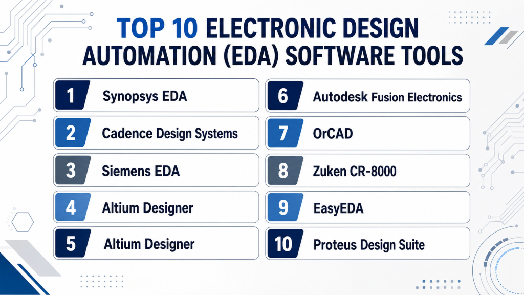
Top 10 Electronic Design Automation (EDA) Software Tools
#1 — Synopsys EDA
Short description (2–3 lines): Synopsys EDA is a leading enterprise-grade EDA portfolio for semiconductor design, verification, IP, software security, and silicon lifecycle workflows. It is best suited for chip companies, SoC teams, advanced semiconductor design houses, and enterprises working on complex silicon products.
Key Features
- IC design and verification workflows
- Logic synthesis and physical design tools
- Formal verification and simulation capabilities
- Semiconductor IP ecosystem
- AI-assisted design optimization options
- Silicon lifecycle management capabilities
- Support for advanced process nodes and large chip programs
Pros
- Very strong for advanced semiconductor and SoC design
- Broad portfolio covering design, verification, IP, and lifecycle
- Strong enterprise adoption in chip design environments
Cons
- Expensive and complex for smaller teams
- Requires skilled engineers and structured implementation
- Not ideal for simple PCB-only workflows
Platforms / Deployment
Linux / Windows for selected tools / enterprise compute environments.
Deployment: Self-hosted / Hybrid / Cloud options vary by product and customer configuration.
Security & Compliance
SSO/SAML, MFA, encryption, audit logs, RBAC: Varies by enterprise configuration.
SOC 2, ISO 27001, GDPR, HIPAA: Not publicly stated.
Integrations & Ecosystem
Synopsys has a broad semiconductor ecosystem covering EDA tools, IP, verification, simulation, and silicon lifecycle workflows. It is typically used in enterprise engineering environments with complex toolchains.
- Semiconductor IP libraries
- Verification and emulation workflows
- Foundry process design kits
- Hardware/software co-design flows
- Enterprise compute and license management
- Integration with internal design management systems
Support & Community
Synopsys provides enterprise support, documentation, training, professional services, and account-based customer assistance. Community access is more enterprise-oriented than casual-user-focused.
#2 — Cadence Design Systems
Short description (2–3 lines): Cadence is a major EDA and computational software provider covering IC design, PCB design, system design, verification, simulation, and AI-assisted engineering workflows. It is widely used by semiconductor companies, electronics manufacturers, and advanced hardware teams.
Key Features
- IC design and verification tools
- PCB design through Allegro and OrCAD families
- System-level design and analysis workflows
- Signal integrity and power integrity analysis
- Verification IP and simulation tools
- AI-driven design and optimization features
- Strong ecosystem for advanced electronics development
Pros
- Broad coverage from chips to boards and systems
- Strong fit for enterprise electronics and semiconductor teams
- Mature ecosystem and strong industry adoption
Cons
- Enterprise tools can be expensive
- Learning curve can be high for advanced flows
- Smaller teams may need simpler packaging or focused tools
Platforms / Deployment
Windows / Linux depending on product.
Deployment: Self-hosted / Hybrid / Cloud options vary by product and customer setup.
Security & Compliance
SSO/SAML, MFA, encryption, audit logs, RBAC: Varies by enterprise deployment and licensing setup.
SOC 2, ISO 27001, GDPR, HIPAA: Not publicly stated.
Integrations & Ecosystem
Cadence has a strong ecosystem across IC, PCB, package, simulation, verification, and system design. It is commonly used in complex electronics workflows where multiple engineering teams must collaborate.
- Allegro and OrCAD PCB workflows
- Virtuoso custom IC design
- Verification and emulation platforms
- Signal and power integrity tools
- Foundry and IP ecosystem
- Enterprise design data workflows
Support & Community
Cadence offers documentation, enterprise support, training, customer portals, partner resources, and formal learning programs. Its community is strong among professional IC, PCB, and semiconductor engineers.
#3 — Siemens EDA
Short description (2–3 lines): Siemens EDA provides a wide range of electronic design automation tools for IC design, verification, PCB design, electronic systems, and manufacturing preparation. It is especially strong for teams that need electronics design connected with manufacturing, digital twin, PLM, and enterprise engineering workflows.
Key Features
- IC design and verification tools
- PCB design and analysis through Xpedition and PADS families
- Design-for-test and manufacturing workflows
- Electronic systems design
- Verification and emulation options
- Digital twin and lifecycle ecosystem alignment
- Strong enterprise integration with Siemens software
Pros
- Strong enterprise ecosystem
- Good fit for electronics teams connected to manufacturing and PLM
- Broad coverage from IC to PCB and system workflows
Cons
- Advanced setup can be complex
- Enterprise licensing may not suit small teams
- Requires planning for full ecosystem value
Platforms / Deployment
Windows / Linux depending on product.
Deployment: Self-hosted / Hybrid / Cloud options vary by product and enterprise configuration.
Security & Compliance
SSO/SAML, MFA, encryption, audit logs, RBAC: Varies by Siemens enterprise configuration.
SOC 2, ISO 27001, GDPR, HIPAA: Not publicly stated.
Integrations & Ecosystem
Siemens EDA connects strongly with Siemens Xcelerator, PLM, manufacturing, simulation, and digital twin workflows. This makes it useful for large companies designing electronics inside broader product systems.
- Xpedition PCB workflows
- PADS PCB design tools
- Teamcenter integration options
- Manufacturing and test workflows
- Verification and emulation platforms
- ECAD-MCAD collaboration
Support & Community
Siemens provides documentation, training, enterprise support, partner resources, and professional services. Support quality depends on package, region, and enterprise agreement.
#4 — Altium Designer
Short description (2–3 lines): Altium Designer is a professional PCB design platform focused on schematic capture, PCB layout, component management, 3D visualization, and electronics product development. It is popular with PCB designers, hardware startups, engineering consultants, and product teams.
Key Features
- Unified schematic and PCB design environment
- Advanced PCB routing and design rule management
- Native 3D PCB visualization
- Component and library management
- ECAD-MCAD collaboration workflows
- Manufacturing output generation
- Cloud collaboration through Altium ecosystem options
Pros
- Strong PCB design experience
- Good usability compared with many enterprise EDA tools
- Useful for professional board design and product teams
Cons
- Can be expensive for small users
- Not a complete advanced IC design platform
- Best value comes when teams use its full PCB workflow
Platforms / Deployment
Windows.
Deployment: Desktop with cloud-connected collaboration options.
Security & Compliance
SSO/SAML, MFA, encryption, audit logs, RBAC: Varies by Altium platform and plan configuration.
SOC 2, ISO 27001, GDPR, HIPAA: Not publicly stated.
Integrations & Ecosystem
Altium has a strong PCB-centered ecosystem with component data, manufacturing outputs, and collaboration features for electronics teams.
- Component libraries and supply-chain data workflows
- ECAD-MCAD collaboration
- Manufacturing outputs
- Cloud collaboration options
- Version control and project sharing workflows
- Integration with mechanical design workflows
Support & Community
Altium provides documentation, tutorials, training content, support plans, forums, webinars, and a large PCB design community. It is generally easier to learn than many full semiconductor EDA stacks.
#5 — KiCad
Short description (2–3 lines): KiCad is a free and open-source EDA suite for schematic capture, PCB layout, 3D board viewing, and manufacturing file generation. It is widely used by hobbyists, startups, educators, open-source hardware teams, and cost-conscious professionals.
Key Features
- Schematic capture
- PCB layout and routing
- 3D PCB viewer
- Symbol and footprint libraries
- Gerber and manufacturing output generation
- Open-source plugin ecosystem
- Cross-platform support
Pros
- Free and open-source
- Strong community and active development
- Good for learning, prototyping, and many professional PCB projects
Cons
- Enterprise support is limited compared with premium tools
- Advanced collaboration and component management may require extra setup
- Some high-end PCB workflows may need commercial alternatives
Platforms / Deployment
Windows / macOS / Linux.
Deployment: Self-hosted desktop.
Security & Compliance
SSO/SAML, MFA, encryption, audit logs, RBAC: Not publicly stated.
SOC 2, ISO 27001, GDPR, HIPAA: Not publicly stated.
Integrations & Ecosystem
KiCad has a strong open-source ecosystem and supports common PCB manufacturing workflows. It is flexible, scriptable, and widely used in community hardware projects.
- Open-source libraries
- Plugin ecosystem
- Gerber file generation
- 3D model support
- Version control through external tools
- Community-maintained extensions
Support & Community
KiCad has strong community support, documentation, forums, tutorials, and open-source contributors. Formal enterprise support is limited, but community learning resources are widely available.
#6 — Autodesk Fusion Electronics
Short description (2–3 lines): Autodesk Fusion Electronics brings schematic design, PCB layout, mechanical integration, and product development workflows into the Fusion environment. It is useful for product teams that need electronics and mechanical design to work together.
Key Features
- Schematic capture
- PCB layout
- Electronics and mechanical design integration
- 3D PCB visualization
- Component library workflows
- Manufacturing output generation
- Cloud-connected collaboration
Pros
- Strong ECAD-MCAD connection
- Useful for product designers and hardware startups
- Good fit when mechanical and electronics teams work closely
Cons
- May not match high-end enterprise PCB or IC design depth
- Some features may require specific subscription levels
- Cloud-connected workflow may not suit every organization
Platforms / Deployment
Windows / macOS.
Deployment: Cloud-connected desktop.
Security & Compliance
SSO/SAML, MFA, encryption, audit logs, RBAC: Varies by Autodesk plan and account configuration.
SOC 2, ISO 27001, GDPR, HIPAA: Not publicly stated.
Integrations & Ecosystem
Fusion Electronics works well when electronics design must connect with mechanical design, product prototyping, and manufacturing workflows.
- Fusion mechanical design workflows
- Autodesk ecosystem
- PCB manufacturing outputs
- Component library workflows
- Cloud project collaboration
- 3D product design workflows
Support & Community
Autodesk provides documentation, community forums, learning resources, and support plans. Fusion has a strong user base among startups, makers, product designers, and small engineering teams.
#7 — OrCAD
Short description (2–3 lines): OrCAD is a PCB design and circuit simulation tool family from Cadence, often used by engineers who need professional schematic capture, PCB layout, and simulation workflows without adopting the full enterprise Allegro environment immediately.
Key Features
- Schematic capture
- PCB layout
- Circuit simulation workflows
- Design rule checking
- Component and library management
- Manufacturing documentation
- Upgrade path into Cadence ecosystem
Pros
- Strong professional PCB design capabilities
- Good stepping stone into the Cadence ecosystem
- Suitable for engineering teams needing more than basic PCB tools
Cons
- Can still have a learning curve for new users
- Advanced enterprise workflows may require Allegro
- Licensing and packaging can require careful review
Platforms / Deployment
Windows.
Deployment: Desktop / enterprise options vary.
Security & Compliance
SSO/SAML, MFA, encryption, audit logs, RBAC: Varies by Cadence configuration.
SOC 2, ISO 27001, GDPR, HIPAA: Not publicly stated.
Integrations & Ecosystem
OrCAD benefits from Cadence’s broader PCB and electronics design ecosystem. It can support teams that may later need more advanced Cadence tools.
- Cadence PCB ecosystem
- SPICE simulation workflows
- Component libraries
- Manufacturing outputs
- Allegro migration path
- Design validation workflows
Support & Community
OrCAD has professional documentation, training resources, Cadence support options, and an established user base. Support levels depend on license and vendor channel.
#8 — Zuken CR-8000
Short description (2–3 lines): Zuken CR-8000 is an advanced PCB and multi-board system design platform for complex electronics development. It is useful for teams building high-density boards, complex systems, automotive electronics, aerospace hardware, and advanced product electronics.
Key Features
- System-level electronics design
- Multi-board design workflows
- PCB layout and routing
- Signal and power integrity support
- 3D product-centric design approach
- Design reuse and constraint management
- Manufacturing preparation workflows
Pros
- Strong for complex PCB and multi-board systems
- Good fit for advanced electronics product companies
- Useful when PCB design must align with system-level planning
Cons
- More specialized than general PCB tools
- May be too advanced for small teams
- Implementation and training require planning
Platforms / Deployment
Windows.
Deployment: Desktop / enterprise options vary.
Security & Compliance
SSO/SAML, MFA, encryption, audit logs, RBAC: Varies / N/A.
SOC 2, ISO 27001, GDPR, HIPAA: Not publicly stated.
Integrations & Ecosystem
Zuken is often used in professional electronics engineering environments where board design, system planning, and manufacturing preparation need to connect.
- ECAD-MCAD workflows
- Manufacturing outputs
- Constraint management
- Multi-board design
- Signal and power integrity workflows
- Enterprise engineering systems
Support & Community
Zuken provides documentation, enterprise support, training, and professional services. Community resources are more specialized compared with tools like KiCad or Altium.
#9 — EasyEDA
Short description (2–3 lines): EasyEDA is a browser-based EDA tool for schematic capture, PCB layout, simulation, and quick board design workflows. It is popular with makers, students, startups, and small teams that want a low-friction online PCB design experience.
Key Features
- Web-based schematic capture
- PCB layout editor
- Component library access
- Simulation options
- Manufacturing output generation
- Collaboration through online projects
- Integration with PCB fabrication ecosystem options
Pros
- Easy to start using
- Good for quick PCB projects and learning
- Browser-based access reduces setup effort
Cons
- Not ideal for advanced enterprise PCB workflows
- Cloud dependency may concern some teams
- Less suitable for complex regulated electronics development
Platforms / Deployment
Web.
Deployment: Cloud.
Security & Compliance
SSO/SAML, MFA, encryption, audit logs, RBAC: Not publicly stated.
SOC 2, ISO 27001, GDPR, HIPAA: Not publicly stated.
Integrations & Ecosystem
EasyEDA is designed for quick PCB design and manufacturing-oriented workflows, especially for users who want fast project setup.
- Online component libraries
- PCB fabrication workflow options
- Gerber outputs
- Browser-based project sharing
- Basic simulation workflows
- Community project examples
Support & Community
EasyEDA has documentation, tutorials, community support, and user examples. It is easier for beginners than many traditional EDA platforms, but formal enterprise support is limited.
#10 — Proteus Design Suite
Short description (2–3 lines): Proteus Design Suite is an electronics design and simulation platform known for schematic capture, PCB layout, and microcontroller simulation. It is widely used in education, embedded systems learning, prototyping, and small electronics design projects.
Key Features
- Schematic capture
- PCB layout
- Microcontroller simulation
- Mixed-mode circuit simulation
- Embedded software and hardware simulation
- Library-based design workflows
- Manufacturing output generation
Pros
- Strong for embedded systems education and prototyping
- Useful microcontroller simulation capabilities
- Good for learning hardware-software interaction
Cons
- Not a complete enterprise IC design platform
- May not be the best fit for high-end PCB production teams
- Ecosystem is smaller than major enterprise EDA providers
Platforms / Deployment
Windows.
Deployment: Desktop.
Security & Compliance
SSO/SAML, MFA, encryption, audit logs, RBAC: Not publicly stated.
SOC 2, ISO 27001, GDPR, HIPAA: Not publicly stated.
Integrations & Ecosystem
Proteus is useful when electronics design needs to connect with embedded software simulation and educational workflows.
- Microcontroller simulation
- PCB layout outputs
- Embedded development workflows
- Component libraries
- Simulation models
- Educational and prototyping use cases
Support & Community
Proteus has documentation, tutorials, support options, and a user base in education and embedded systems. Community strength is good in learning environments but more limited for enterprise semiconductor design.
Comparison Table
| Tool Name | Best For | Platform(s) Supported | Deployment (Cloud/Self-hosted/Hybrid) | Standout Feature | Public Rating |
|---|---|---|---|---|---|
| Synopsys EDA | Advanced semiconductor and SoC design | Linux, Windows for selected tools | Self-hosted / Hybrid / Cloud options vary | Full enterprise silicon design and verification portfolio | N/A |
| Cadence Design Systems | IC, PCB, package, and system design | Windows, Linux depending on product | Self-hosted / Hybrid / Cloud options vary | Broad EDA coverage from chips to systems | N/A |
| Siemens EDA | Enterprise electronics and manufacturing-connected workflows | Windows, Linux depending on product | Self-hosted / Hybrid / Cloud options vary | EDA connected with digital twin and PLM workflows | N/A |
| Altium Designer | Professional PCB design teams | Windows | Desktop + cloud-connected options | Unified PCB design with 3D visualization | N/A |
| KiCad | Open-source PCB design and prototyping | Windows, macOS, Linux | Self-hosted desktop | Free open-source PCB design suite | N/A |
| Autodesk Fusion Electronics | Product teams needing ECAD-MCAD connection | Windows, macOS | Cloud-connected desktop | Electronics and mechanical design in one environment | N/A |
| OrCAD | Professional PCB and circuit design | Windows | Desktop / enterprise options vary | Strong PCB design with Cadence ecosystem path | N/A |
| Zuken CR-8000 | Complex PCB and multi-board systems | Windows | Desktop / enterprise options vary | System-level and multi-board electronics design | N/A |
| EasyEDA | Beginners, makers, quick PCB projects | Web | Cloud | Browser-based PCB design and quick fabrication workflow | N/A |
| Proteus Design Suite | Embedded systems learning and simulation | Windows | Desktop | Microcontroller and circuit simulation | N/A |
Evaluation & Scoring of Electronic Design Automation (EDA) Software
The scoring below is comparative. It is based on practical product depth, adoption, usability, ecosystem strength, security signals, support availability, and buyer value. It is not a public review rating.
| Tool Name | Core (25%) | Ease (15%) | Integrations (15%) | Security (10%) | Performance (10%) | Support (10%) | Value (15%) | Weighted Total (0–10) |
|---|---|---|---|---|---|---|---|---|
| Synopsys EDA | 10 | 4 | 9 | 8 | 9 | 9 | 5 | 7.95 |
| Cadence Design Systems | 10 | 5 | 9 | 8 | 9 | 9 | 6 | 8.20 |
| Siemens EDA | 9 | 5 | 9 | 8 | 9 | 8 | 6 | 7.95 |
| Altium Designer | 8 | 8 | 8 | 7 | 8 | 8 | 7 | 7.80 |
| KiCad | 6 | 7 | 6 | 4 | 6 | 7 | 10 | 6.60 |
| Autodesk Fusion Electronics | 7 | 8 | 8 | 7 | 7 | 8 | 8 | 7.55 |
| OrCAD | 8 | 6 | 8 | 7 | 8 | 8 | 7 | 7.45 |
| Zuken CR-8000 | 8 | 5 | 8 | 7 | 8 | 7 | 6 | 7.05 |
| EasyEDA | 5 | 9 | 6 | 4 | 6 | 6 | 9 | 6.35 |
| Proteus Design Suite | 6 | 7 | 6 | 4 | 6 | 6 | 8 | 6.20 |
How to interpret the scores:
- Higher scores show stronger overall fit across the selected criteria, not a universal winner.
- Enterprise EDA platforms score high in depth, performance, support, and ecosystem, but lower in ease and price/value for small teams.
- PCB-focused tools often score better in usability and practical adoption for hardware teams.
- Open-source and browser-based tools can offer strong value but may not match enterprise governance or advanced verification depth.
- Final selection should depend on design complexity, team skill, compliance needs, fabrication workflow, and integration requirements.
Which Electronic Design Automation (EDA) Software Tool Is Right for You?
Solo / Freelancer
Solo engineers, consultants, and independent designers should focus on cost, ease of use, file outputs, component libraries, and client compatibility.
Good options include:
- KiCad for open-source PCB design and low-cost professional work
- EasyEDA for quick browser-based PCB projects
- Autodesk Fusion Electronics for combined product and electronics design
- Proteus Design Suite for embedded simulation and learning-focused work
- Altium Designer if the freelancer works with professional clients that require stronger PCB deliverables
A solo user usually does not need Synopsys, Cadence full-stack EDA, or Siemens enterprise flows unless working directly on semiconductor or large enterprise projects.
SMB
Small and medium electronics companies need practical PCB design, component management, manufacturing outputs, and some collaboration.
Good options include:
- Altium Designer for serious PCB design teams
- OrCAD for professional PCB and circuit workflows
- Autodesk Fusion Electronics for hardware product teams needing ECAD-MCAD workflows
- KiCad for cost-sensitive teams with strong internal skill
- Zuken CR-8000 for more complex board and system designs
SMBs should check whether the tool supports their manufacturer’s preferred outputs, whether libraries are manageable, and whether collaboration features are enough for the team size.
Mid-Market
Mid-market companies usually need design governance, reusable libraries, version control, review workflows, supply-chain visibility, and better integration with mechanical and manufacturing teams.
Good options include:
- Altium Designer for PCB-focused teams
- OrCAD or Cadence Allegro workflows for growing electronics teams
- Siemens EDA for companies already using Siemens engineering tools
- Zuken CR-8000 for complex PCB and multi-board products
- Autodesk Fusion Electronics for product teams with mechanical integration needs
Mid-market buyers should pay attention to library control, design release process, permission models, integration with PLM, and supplier collaboration.
Enterprise
Enterprise buyers often need advanced verification, IC design, package design, large-scale PCB design, PLM integration, security governance, and long-term support.
Good options include:
- Synopsys EDA for advanced semiconductor and SoC design
- Cadence Design Systems for IC, PCB, package, and system workflows
- Siemens EDA for electronics design tied to manufacturing, PLM, and digital twin workflows
- Zuken CR-8000 for complex system-level PCB design
- Altium Enterprise ecosystem options for distributed PCB teams needing collaboration and control
Enterprise teams should run technical pilots using real design data, not demo projects only. Security, export control, IP protection, tool interoperability, and license governance should be part of the buying process.
Budget vs Premium
For budget-sensitive users, KiCad, EasyEDA, and selected lower-cost PCB tools are practical starting points. They are useful for learning, prototyping, and many small PCB designs.
For premium workflows, Synopsys, Cadence, Siemens EDA, Altium Designer, and Zuken CR-8000 are stronger choices. Premium tools make more sense when design risk, verification needs, compliance pressure, or production scale is high.
Feature Depth vs Ease of Use
If ease of use matters most, consider EasyEDA, KiCad, Autodesk Fusion Electronics, or Altium Designer.
If deep engineering capability matters more, consider Synopsys, Cadence, Siemens EDA, Zuken CR-8000, or OrCAD.
A beginner-friendly tool is not always enough for regulated electronics, high-speed design, or semiconductor work. At the same time, an enterprise platform may be unnecessary for simple board design.
Integrations & Scalability
EDA tools do not work alone. They often connect with mechanical CAD, PLM, ERP, simulation tools, fabrication partners, source control systems, and component databases.
Strong integration scenarios include:
- Altium Designer for PCB design and ECAD-MCAD collaboration
- Autodesk Fusion Electronics for product design teams using mechanical workflows
- Siemens EDA for Siemens PLM and digital manufacturing ecosystems
- Cadence for IC, package, and board-level design flows
- Synopsys for semiconductor verification, IP, and silicon lifecycle workflows
- KiCad with Git and open-source workflows for flexible collaboration
Scalability should include design size, user count, file management, library governance, support, and licensing flexibility.
Security & Compliance Needs
EDA files are highly sensitive because they often contain product IP, circuit designs, chip architectures, firmware interfaces, and manufacturing data. Security should be reviewed before purchase, especially for cloud or supplier-facing workflows.
Important controls include:
- SSO and MFA
- Role-based access control
- Audit logs
- Encryption
- Project-level permissions
- Secure external sharing
- IP protection controls
- Backup and recovery process
- Export control support where relevant
- Vendor security documentation
For regulated industries such as automotive, aerospace, defense, medical devices, and semiconductor design, security and compliance review should be part of the selection process from the beginning.
Frequently Asked Questions (FAQs)
What is Electronic Design Automation software?
Electronic Design Automation software helps engineers design, simulate, verify, and prepare electronic products for manufacturing. It is used for PCB design, IC design, chip verification, circuit simulation, and related electronics workflows.
Is EDA software only for semiconductor companies?
No. EDA software is used by semiconductor companies, PCB designers, embedded engineers, hardware startups, electronics manufacturers, universities, and research teams. The right tool depends on whether the work is chip design, board design, or system-level electronics.
Which EDA software is best for beginners?
KiCad, EasyEDA, Proteus, and Autodesk Fusion Electronics are common beginner-friendly options. They are easier to start with than advanced enterprise semiconductor platforms.
Which EDA software is best for PCB design?
Altium Designer, KiCad, OrCAD, EasyEDA, Autodesk Fusion Electronics, Zuken CR-8000, and Siemens PCB tools are common PCB design options. The best choice depends on complexity, budget, collaboration needs, and manufacturing workflow.
Which EDA software is best for IC and semiconductor design?
Synopsys, Cadence, and Siemens EDA are common choices for advanced IC, ASIC, SoC, and semiconductor workflows. These platforms are usually used by experienced teams with formal engineering processes.
What pricing models are common in EDA software?
EDA tools may use subscriptions, floating licenses, named-user licenses, enterprise contracts, cloud credits, or module-based pricing. Open-source tools may be free, but support and training still require time and effort.
What are common mistakes when choosing EDA software?
Common mistakes include choosing only by price, ignoring manufacturing outputs, skipping library governance, underestimating training, and not testing real project files during evaluation.
How long does EDA implementation take?
Small PCB teams can start quickly with lightweight tools. Enterprise IC, PCB, or system design environments may need longer onboarding because of licensing, compute setup, libraries, templates, security controls, and workflow integration.
Is cloud EDA safe?
Cloud EDA can be safe when proper controls are available and configured correctly. Buyers should check SSO, MFA, encryption, audit logs, data storage rules, access control, and external sharing policies.
Can I switch from one EDA tool to another easily?
Switching is possible but not always simple. Libraries, symbols, footprints, constraints, simulation models, scripts, and manufacturing outputs may need conversion and validation.
Are open-source EDA tools good enough?
Open-source tools like KiCad can be very useful for learning, prototyping, and many professional PCB projects. For advanced semiconductor design, regulated product development, or enterprise workflows, commercial tools may offer stronger support and deeper capabilities.
Do EDA tools integrate with mechanical design software?
Many modern EDA tools support ECAD-MCAD workflows, 3D board views, STEP export, enclosure checks, and collaboration with mechanical teams. This is important for products where board shape, connectors, heat, and enclosure fit matter.
What is the difference between PCB EDA and IC EDA?
PCB EDA focuses on schematic capture, board layout, routing, and manufacturing files. IC EDA focuses on chip architecture, logic design, verification, physical design, timing, power, and semiconductor manufacturing preparation.
How should a company evaluate EDA software before buying?
A company should shortlist tools, run a pilot with real design files, check library workflows, validate manufacturing outputs, test integrations, review security controls, and compare total cost over multiple projects.
Conclusion
Electronic Design Automation software is a critical foundation for modern electronics development, but the best tool depends strongly on the type of work being done. A hardware startup designing PCBs has very different needs from a semiconductor company building advanced SoCs. KiCad, EasyEDA, Proteus, and Autodesk Fusion Electronics can be practical for learning, prototyping, and smaller teams. Altium Designer, OrCAD, and Zuken CR-8000 are stronger for professional PCB and product electronics workflows. Synopsys, Cadence, and Siemens EDA are better suited for advanced semiconductor, verification, enterprise electronics, and system-level design environments.